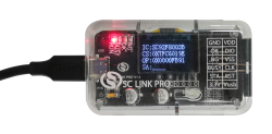
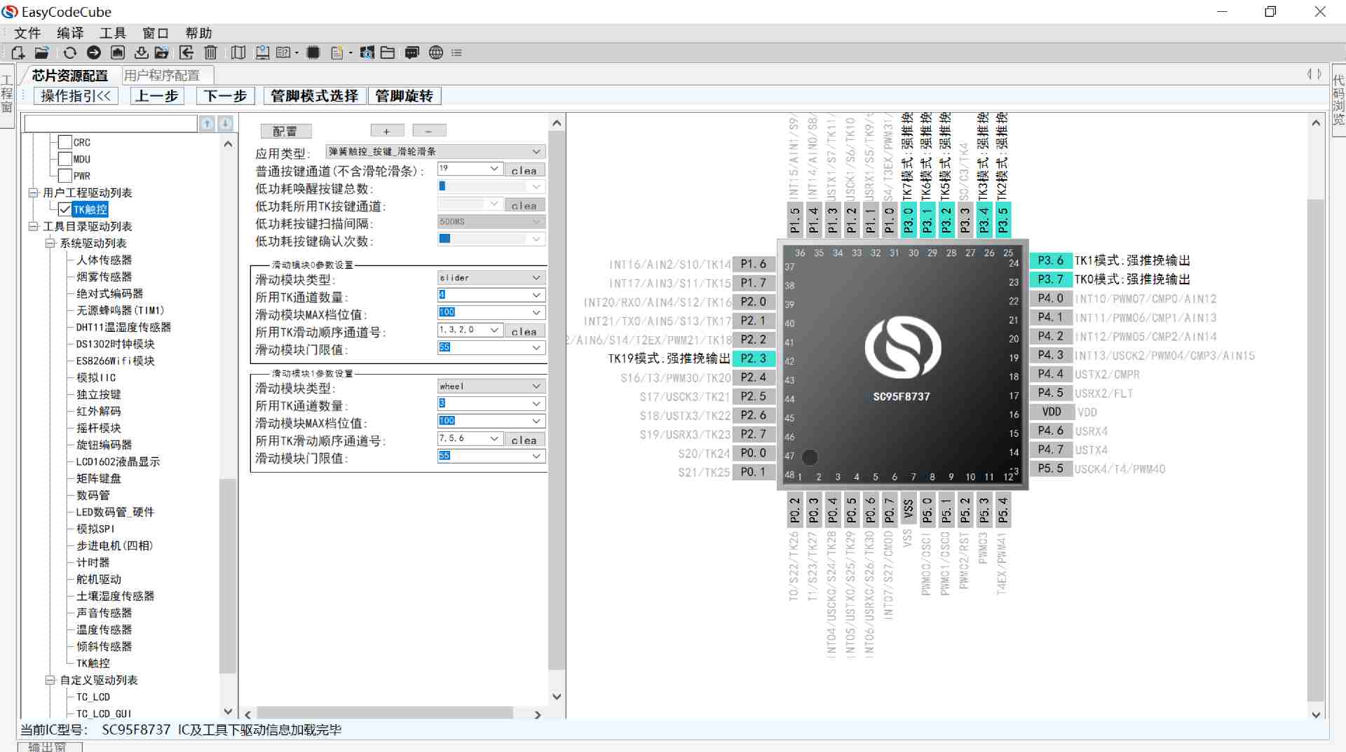
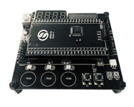
SC LINK PRO is designed for offline/online programming & simulation and TouchKey debugging of SC92F/93F/95F series MCU
Products
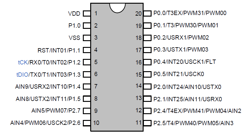
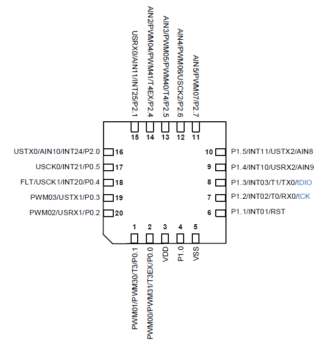
SC95F7672
Operating Conditions
l Voltage Range: 2.0V~5.5V
l Temperature Range: -40℃ ~ +105℃
CPU
l Super-high-speed 1T 8051 core
l The instruction set compatible with 8051
l The execution speed is about twice that of other 1T 8051
l Double data pointers (DPTRs)
Flash ROM
l 64 Kbytes Flash ROM
l Can be rewritten 100,000 times
l APROM area allowed IAP operation in Flash can be set to 0K/1K/2K/All APROM by Code Option.
LDROM
l BootLoader code memory
l LDROM area can be set to 0K/1K/2K/4K by Code Option
EEPROM
l Independent 6K bytes EEPROM
l Can be rewritten 100,000 times, has more than 100-year preservation life in the ambient temperature of 25℃
SRAM
l 256 bytes on-chip direct access RAM
l 4 Kbytes on-chip Indirect access RAM
l PWM RAM
Flash Programming and Emulation
l 2-wire JTAG programming and emulation interface
System clock (fSYS)
l Built-in high frequency 32 MHz oscillator (fHRC)
n can be selected and set by the programmer as: 32/16/8/4 MHz@2.0~5.5V
n Frequency Error: Within ±1% @ -40 ~ 105℃ @ 2.0 ~ 5.5V
Built-in high-frequency crystal oscillator circuit:
l Can be connected with external 2~16MHz oscillator
l As the system clock source, fSYS has the programmer option to use one of the four frequency splits of external crystal / 1/2/4/8
l The built-in system clock monitoring circuit. If you select a crystal oscillator as the system clock source and the crystal oscillator circuit stops, the system clock source automatically switches to the built-in HRC and stays in this state until reset next time
Built-in low-frequency 32 kHz oscillator (LRC):
l used as the clock source for Base Timer and wake up STOP
l used as the clock sourse for WDT
l Frequency Error: After the register correction, within ±4% @ -20 ~ 85℃ @ 4.0 ~ 5.5V
Low-voltage Reset (LVR)
l 4 options of reset voltage: 4.3/3.7/ 2.9/1.9V
l the default value can be selected by the Code Option
Interrupts (INT)
l Timer 0~Timer 4, INT0~2, ADC, PWM, UART, USCI0~2, Base Timer 15 interrupt sources
l External interrupt contains 3 interrupt vectors, 13 interrupt ports. All can set up rising edge, falling edge, dual edge interrupt
l Two-level interrupt priority capability
Digital Peripheral
l GPIO: Up to 18 bidirectional independently controllable I/O ports
n Independent setting of pull-up resistors
n ALL GPIO source drive capacity is controlled by four levels
n All IO ports have large sink current drive capability (50mA)
l Built-in WDT, optional clock frequency division ratio
l 5 Timers: Timer0~4
n Time2、Timer3 and Timer4 have Capture function
n Time2、Timer3 and Timer4 each can provide two conventional PWM
l 4-channel 16-bit conventional PWM
n Time2、Timer3 and Timer4 each can provide two conventional PWM
l 8-channel 16-bit multi-function PWM
n Public cycle and the duty cycle can be set separately
n Complementary PWM waveforms with dead zones can be output
n Models in pin packages of 20PIN and above support PWM Fault Detection (FLT)
l One independent UART communication port UART0
l 3 UART/SPI/TWI communication interfaces (USCI)
n When USCI0 is set to SPI0, the driving capability of the pins corresponding to its signal port will be enhanced
l Built-in CRC check module
l Integrated with 16 * 16-bit hardware Multiplier-Divide Unit (MDU)
Analog Peripheral
l 9-channel 12-bit ADC
n Build-in reference voltage of 2.048V, 1.024V and 2.4V
n The ADC reference voltages is optional: VDD, internal 2.048V, internal 1.024V and 2.4V
n 1 internal channel can measure the voltage of the power supply
n ADC conversion complete interruption can be set
Power Saving Mode
l IDLE Mode: can be woken up by any interrupt
l STOP Mode: can be woken up by INT0~2 Base Timer.
