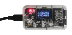
SC LINK PRO is designed for offline/online programming & simulation and TouchKey debugging of SC92F/93F/95F series MCU
Products
SC32F10GK8QJR
1 Features
Operating Conditions
l Operating voltage: 2.0V~5.5V
l Operating temperature: -40 ~ +105℃
EMS
l ESD
n HBM:MIL-STD-883J Class 3B
n MM:JEDEC EIA/JESD22-A115 Class C
n CDM:ANSI/ESDA/JEDEC JS-002-2018 Class C3
l EFT
n EN61000-4-4 Level 4
Package
l 32 PIN: QFN32 (5X5)
Core
l With Wakeup Interrupt Controller (WIC) module
l 64-bits instruction prefetch
l Built-in Multiplier Unit (MDU)
Reset
l Power-On Reset (POR)
l Software Reset
l Reset through external NRST pin (PC1) with a low-level signal
l Watchdog Timer (WDT) reset
l Low Voltage Reset (LVR)
n Four selectable reset voltages: 4.3V, 3.7V, 2.9V, 1.9V
n The default value is determined by the user's programmed Code Option
BUS
l 1 IOPORT
l 1 AHB
l 3 APB:APB0~APB2
Power Saving Mode
l IDLE Mode,can be woken up by any interrupt
l STOP Mode,can be woken up by INT0~15, Base Timer, TK, and CMP
1.1 Flash
APROM
l Up to 256 Kbytes APROM
l Can be rewritten up to 100,000 times
l Supports hardware read protection encryption
l Supports hardware write protection: Provides two regions for disabling IAP (In-Application Programming) operations. Users can configure the settings through the Code Option, with the minimum setting unit being 512 bytes (one sector)
LDROM
l 2 Kbytes of system storage area, factory-programmed with BootLoader program
SRAM
l 8 Kbytes Internal SRAM
l Supports booting from SRAM
96 bits unique ID
l 96-bit Unique ID defined in the design option area
1.2 BootLoader
l Hardware method: System storage area of 2 Kbytes, factory-programmed with BootLoader program
l Software method: Supports interrupt vector table remapping, allowing flexible partitioning of the APROM area for user BootLoader program execution
1.3 Flash Programming and Emulation
l Programming methods supported: ICP / ISP / IAP
l 2-wire JTAG / SWD programming and emulation interface
l Simulation functionality is not supported in encrypted mode
1.4 Clock source
Built-in high-frequency 32 MHz oscillator (HIRC)
l Can be selected as the system clock source
l Can be selected as the PLL clock source
l Frequency Error: Within ±1% @ -40 ~ 105℃ @ 2.0V~ 5.5V
l The system clock can be automatically calibrated by 32.768 kHz external crystal oscillator, after calibration HIRC accuracy can be infinitely close to the accuracy of external 32.768 kHz crystal oscillator
Built-in low-frequency 32 kHz oscillator (LIRC)
l Can be selected as the system clock source
l Fixed as the WDT clock source, which is always enabled when WDT is enabled
l Can be selected as the Base Timer clock source
l Can be selected as the LCD/LED clock source
l Frequency Error: Within ±4% @ -20 ~ 85℃ @ 4.0V~ 5.5V, after register correction
External 2~16MHz crystal oscillator (HXT)
l Can be selected as the system clock source
l Can be selected as the PLL clock source
l User can choose an external crystal oscillator oscillating frequency of <12MHz or ≥12MHz
External 32.768 KHz crystal oscillator (LXT)
l Can be selected as the system clock source
l Can be selected as the Base Timer clock source
l Can be selected as the LCD/LED clock source
l Allows for an external 32.768kHz oscillator
l Automatic calibration of HIRC can be performed using LXT
PLL
l Can be selected as the system clock source
l The PLL clock source can be selected from HIRC or HXT
l The maximum output frequency of PLLRCLK is 64MHz, which can serve as the system clock
1.5 Interrupts (INT)
l Up to 27 interrupts
l Four-level interrupt priority can be set
n 16 interrupts, occupying 4 interrupt vectors in total
n Change Interrupts on All GPIO pins
n All interrupts can be set as rising edge, falling edge, or both-edge interrupts, each with an independent corresponding interrupt flag
n Setting the corresponding interrupt flag in software triggers entry into the corresponding interrupt
1.6 Digtal peripherals
Up to 30 GPIOs
l Independent pull-up resistor configuration is available
l All GPIO pins have source driving capability controlled by four levels
l All GPIO pins have high sink current driving capability (50mA)
Watchdog timer (WDT)
l Built-in WDT with programmable overflow time ranging from 3.94ms to 500ms
Base Timer(BTM)
l The clock sources LXT and LIRC are selectable
l Selectable interrupt frequency intervals from 15.625ms to 32s
l Can wake up from STOP Mode
8 16-bit timers: Timer0~Timer7
l 16-bit up, down, and up/down auto-reload counters
l Supports rising edge/falling edge capture for PWM duty and period capture
l TIM1~7 can provide individually adjustable PWM (TnPWMA) with controllable duty cycle through the Tn port
l TIM0 can provide individually adjustable PWM (TnPWMB) with controllable duty cycle through the TnEX port
l TIM1/2/6 timer overflow and capture events can trigger DMA requests
l TIM2/3/7 Tn pins support remapping
5 channels 16-bit Advanced PWM0
l The clock source can be selected up to 64MHz
l Shared period and independently adjustable duty cycle
l Support dead time and complementary PWM output
l Support fault detection
17 channels 8-bit LEDPWM
l Shared period and independently adjustable duty cycle
l Support center-aligned mode
l Support fault detection
4 independent UART: UART0~3
l UART2 can be mapped to another set of IO pins
l Independent baud rate generator
l Support wake-up from STOP Mode
l Three communication modes available
n Mode 0: 8-bit half-duplex synchronous communication
n Mode 1: 10-bit full-duplex asynchronous communication
n Mode 3: 11-bit full-duplex asynchronous communication
l UART0 and UART1 support DMA requests
l UART2 and UART3 do not support DMA requests
2 independent SPI: SPI0/SPI1
l SPI0:
n A 16-bit 8-level FIFO with separate transmit and receive
n Can be mapped to two additional sets of ports
n Supports DMA
l SPI1:
n Can be mapped to another set of ports
n Supports DMA
2 independent TWI: TWI0/TWI1
l Supports master mode or slave mode
l Supports clock stretching in slave mode
l Communication speed of up to 1Mbps
l TWI0 supports DMA
CRC
l Initial value can be set, with a default of 0xFFFF_FFFF
l Polynomial can be programmed, with a default of 0x04C1_1DB7
l Supports 8/16/32-bit data units
LCD/LED Driver
l The clock sourses LXT and LIRC are selectable
l LCD/LED selection, sharing registers and ports
l LED
n 4 X 20 segment LED drivers
n LED segment port source drive capability divided into four levels of control
n Registers shared with 32-channel LEDPWM, enabling LED replacement drive and grayscale adjustment through center-aligned PWM waveforms
l LCD
n 4 X 20 segment LCD drivers
n Selectable voltage divider resistance for LCD voltage output port
n Choice of two bias voltages: 1/3 and 1/4
n Two waveform modes, Type A and Type B, are available
n Three frame frequencies to choose from:32 Hz to 128 Hz under Type A mode
l The clock sources LXT and LIRC are selectable
l LCD and LED are mutually exclusive options, sharing registers and ports
l LED:
n Supports 4 X 20 segment LED driving
n LED segment port has source driving capability controlled by four levels
n Shares registers with 32-channel LEDPWM, allowing LED replacement driving and grayscale adjustment through center-aligned PWM waveforms
l LCD:
n Supports 4 X 20 segment LCD driving
n LCD voltage output port has selectable voltage divider resistor values
n Two bias voltages options: 1/3 and 1/4
n Two waveform modes: Type A and Type B
n Three frame frequencies available: 32 Hz to 128 Hz in Type A mode
DMA
l 4 independent configurable channels
l Each DMA channel can send DMA requests to other channels
l Data width supports byte, half-word, and word
l 24 DMA request sources with four priority levels
l Supports source/destination address auto-increment or fixed
l Supports single and burst transfer modes
l Transfer modes: memory to memory, memory to peripheral, peripheral to memory, peripheral to peripheral
1.7 Analog peripherals
Analog-to-Digital Converter ADC
l Precison: 14 bits
l Supports up to 9 channels
l External 8 ADC sampling channels can be multiplexed with I/O ports for other functions
l One internal ADC can directly measure VDD voltage
l Four options for ADC reference voltage: VDD, and internal 2.048V, 1.024V, or 2.4V
l Configurable ADC conversion completion interrupt
l Supports single-channel continuous conversion mode
l Supports DMA
Analog Comparator CMP
l Four analog signal positive input terminals: CMP0~CMP3
l Negative input voltage can be selected from CMPR handover or one of the 16 comparison voltages derived from the internal VDD voltage division
l CMP interrupts can wake up the STOP mode